VLSI PDA - Physical Design Introduction
參考清大王廷基老師課程講義
IC Design Flow
System Specification
定義系統的需求,例如:功耗、面積、效能、功能等等。
Functional Design
定義系統的功能,例如:模擬、驗證、合成等等。
Logic Synthesis
把功能描述轉換成電路描述,並做邏輯上的優化,例如:RTL、Netlist。
Circuit Design
早期才有,這些 Logic Gate 要用那些 Transistor 來做。現在都用
Cell Based Design,從Cell Library拿標準元件來做,這些元件的 Layout 都已經設計好了。Physical Design
Fabrication
Packaging & Testing
Physical Desgin
把 Circuit Netlist 轉換成 Layout 的過程,每個元件要擺哪、要怎麼連接、怎麼樣才能達到最佳的 Power, Performance, Area (PPA),甚至於 Security。
Computer-Aided Design (CAD)
- CAD 是一個廣泛的領域,包含了各種不同的應用,例如:電路設計、機械設計、建築設計、電子設計等等。
- EDA 是 CAD 的一個子集,專門用來設計電子電路。
Physical Design Flow
- Partitioning
將整個設計拆分成較小的模組或區塊,以便於後續的設計。 - Floorplanning
確定各個功能模組 (Functional Unit Block) 的位置 - Placement
將標準單元(Standard Cells)、IPs 放到前面的 Functional Unit Block 裡面,常常跟 Floorplanning 一起做。 - Clock Tree Synthesis
讓所有 Clock 訊號能夠同步傳遞到各個元件 - Routing
根據 Netlist 和 Placement 的資訊,把元件之間的連線接起來 - Post-routing Optimization
- Compaction
早期才有,把 Placement 的結果做最佳化,現在都直接在 Placement 決定面積要多大 - Extraction & Verification
不同步驟之間常常會有 feedback loop
IP (Intellectual Property)
- Hard IP
通常是一個完整的功能模組,例如:CPU、GPU、DDR Controller - Soft IP
通常是一個功能模組的 RTL Code,Layout 還沒決定,可以根據不同的製程和需求做修改
Moore’s Law
每隔 18-24 個月,晶片上的元件數量會增加一倍
More Moore
依賴於先進製程技術的推進(7nm → 5nm → 3nm → 2nm)。
- FinFET → GAAFET(環繞閘極電晶體)→ CFET (互補場效應電晶體)
- EUV (Extreme Ultraviolet Lithography)
- 先進封裝技術,Chiplet、3D IC
More than Moore
專注於縮小電晶體尺寸
- Compute-in-Memory
VLSI Design Considerations
- Design Complexity
- Performance
- Time-to-Market
- Cost: Die Area, Packaging, Testing
- Power Consumption、Noise、Reliability
考慮到不同的目標,會有不同的設計方法,像是:Full Custom Design, Standard Cell Design, Gate Array Design, FPGA, CPLD, SPLD, SSI
Full Custom Design
完全自訂,可以達到最佳的 PPA,但是花費時間和金錢最多
Standard Cell Design
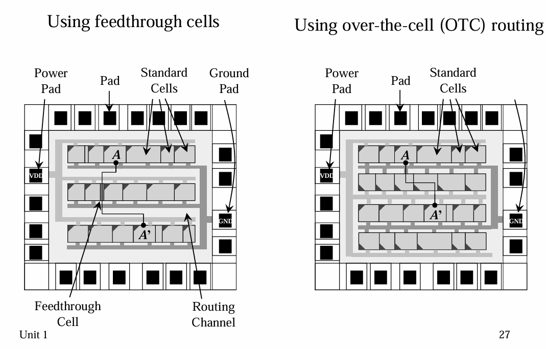
有一個 Cell Library,裡面有很多標準元件,每個都有固定的高度。Layout 都已經設計好了,只要做 Metal Layer 就好
早期 Metal 層數不多,可以留 Routing Channel、Feedthrough Cell 來連接不同的 Cell。現在層數比較多,連線都在上空,所以可以把整 Row 的 Cell 翻轉,讓 GND 在一邊、VDD 在另一邊,減少 Routing 的複雜度
Gate Array Design
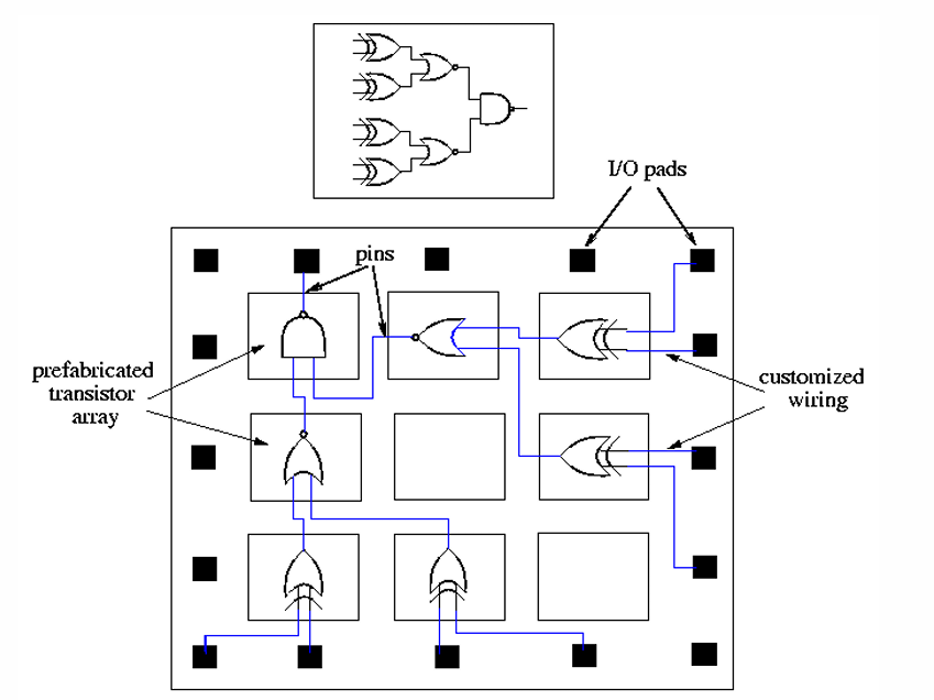
Cell 裡面、Cell 之間的連線都沒有決定,可以根據需求來做 (沒什麼人在用?
FPGA (Field Programmable Gate Array)
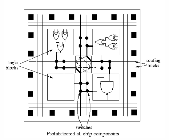
可以決定每個 Cell 的功能,線也連好了,線可以用 Switch、Switch Box 控制
LUT (Look-Up Table)
把某個計算過程的所有 Input 組合對應的 Output 存起來,這樣就不用每次都重新計算
SPLD (Simple Programmable Logic Device)
比 FPGA 簡單,只有一個矩陣,沒有 LUT
Comparison
| Full Custom | Standard Cell | Gate Array | FPGA | SPLD | |
|---|---|---|---|---|---|
| Cell Size | variable | fixed height | fixed | fixed | fixed |
| Cell Type | variable | variable | fixed | programmable | programmable |
| Cell Placement | variable | in row | fixed | fiexed | fixed |
| Interconnections | variable | variable | variable | programmable | programmable |
高度的單位通常用 Track (T) 表示。因為 Standard Cell 的高度不是固定的,有些是 5 Track、有些是 7 Track,所以在做 Placement 的時候要考慮這些高度不同的 Cell (哪些 Row 要放某種高度的 Cell 之類的)
| Full Custom | Standard Cell | Gate Array | FPGA | SPLD | |
|---|---|---|---|---|---|
| Fabrication Time | — | – | + | +++ | ++ |
| Packing Density | +++ | ++ | + | – | — |
| Unit Cost in Large Quantity | +++ | ++ | + | – | - |
| Unit Cost in Small Quantity | — | – | + | +++ | ++ |
| Easy Desgin and Simulation | — | – | - | ++ | + |
| Easy Desgin Change | — | – | - | ++ | ++ |
| Accuracy of Timing Simulation | - | - | - | + | ++ |
| Chip Speed | +++ | ++ | + | - | – |
Macro Cells
Macro 是常常用到的,很大片的 Logic Cell,可能包含很多個 Standard Cell,例如:ALU、Multiplier、Memory
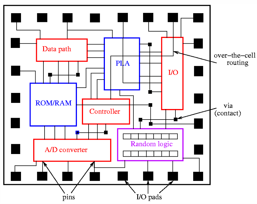
Structured ASIC (Application Specific Integrated Circuit)
- ASIC
專門為某個應用設計的晶片,常常被用來跟 FPGA 做區隔,不是 FPGA 的就稱為 ASIC
Structured ASIC 介於 FPGA 和 Gate Array 之間,會事先定義好一些 Metal Layers 和 Via Layers (Cut Layers),剩下的 Layers 都是 Customizable,根據需求來客製化。很適合 ECO (Engineering Change Order),只要改 Customizable 的部分就好
越低層的 Layer 的線會比較細,RC 特性比較差,Timing 也會比較差,Delay 比較大。反之,越高層的 Layer,線會比較粗,Delay 比較小,因此越重要的 Signal 會放在越高層的 Layer
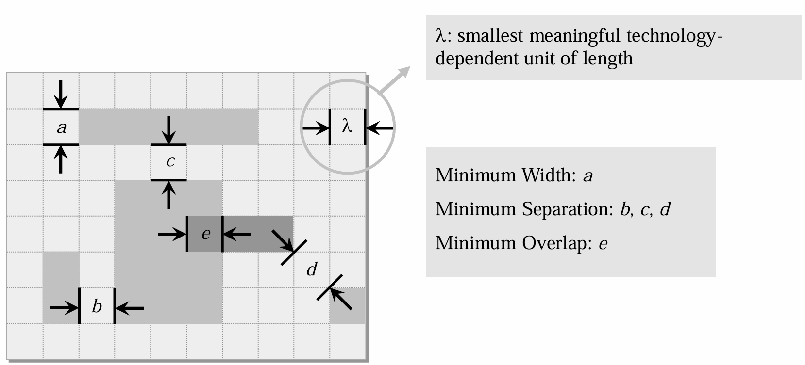
Design Rules
Size Rules
限制最小的長度、寬度Seperation Rules
限制元件之間最小的間距,可能是同一層或相鄰層,可能是 Rectilinear、Euclidean diagonal distance,避免短路。Spacing 的部分不是常數,會隨著與相鄰 (不同 Track) Metal 重疊的部分有所不同Overlap Rules
限制元件之間的重疊的最小面積。每一層 Layer 會有不同的光罩,有時候會有誤差,所以會需要一些 Overlap 來保護